

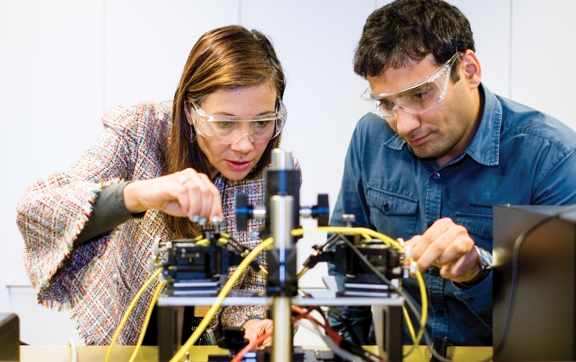
Electronics engineer Francesca Iacopi is intent on taking innovative 2D materials like graphene out of the lab and into the realm of everyday use.
Novel ‘wonder materials’ with incredible promise can grab attention and the imagination. Harnessing the promise of any physics or chemistry breakthrough, however, takes time.
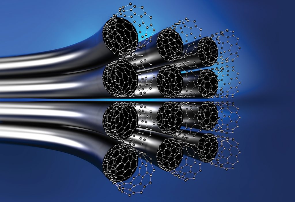
This has been the case with graphene. First isolated in 2004 and earning a Nobel Prize in 2010 for the two University of Manchester researchers responsible for it, the substance led to many articles focusing on its incredible conductivity and strength, as well as huge research investments. These include thousands of patents filed internationally and the launch of the €1 billion Graphene Flagship initiative in the European Union.
But high-end commercial applications have been elusive. Most graphene products so far are materials such as coatings and dyes, or composites for high-performance sports equipment, such as tennis racquets and bicycles. With graphene, the bridge from laboratory to real-world application can be long, and it is there where Professor Francesca Iacopi, FIEAust, operates.
Iacopi heads the INSys Lab at the University of Technology Sydney and said a lot of the focus in the world of graphene — a family of materials based on a single layer of hexagonally arranged carbon atoms — remains on the fundamentals of the material and its devices, which is key groundwork.
“I come from industry, before turning into an academic,” she told create.
“Most of my career has been in R&D, and so I’m very well aware of the years-long lag that exists between having a nice idea in the lab and getting to something that actually can be scaled up and can be reproducible and incorporated into a high-end product that can be actually used.
“It’s very rewarding work, and I’ve gone through that cycle a couple of times in my career, but it takes time.”

In Australia, graphene research takes on a number of different flavours, notes Iacopi, and areas of research excellence include the University of Adelaide, the University of Wollongong and Deakin University. Her group’s focus is on the material’s integration into miniature electronics devices.
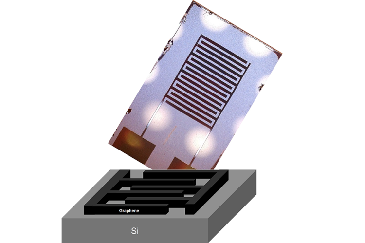
Some of the academic community working with graphene has moved on to newer 2D materials. Iacopi’s group looks at these, too, but Iacopi is most interested in the long game of industrialising graphene. A major contribution she has made to this task is her 2014 invention of a platform technology for producing high-quality graphene on silicon wafers, using solid-source growth from silicon carbide films produced by epitaxy.
This method lends itself to current industrial processes in the semiconductor industry.
“The advantage of that is if you’re able to synthesise graphene directly on the silicon wafers, you are basically on the highway to integrate that material with the existing technologies,” she said.
“But it’s not a short-term sort of endeavour. It really takes a lot of time and effort … I’m really trying to keep the momentum going specifically on graphene, among others, because I want to demonstrate that graphene can be used in high-end applications, as opposed to exclusively as a composite.”
Graphene on silicon
The process, which Iacopi developed at Griffith University in 2014, was used early on to create micro-resonators. She is most interested in developing miniaturised devices using the platform, which could have a broad range of applications.
“We are looking into electronics, but we are also looking into energy storage — so miniaturised, integrated energy storage,” Iacopi said.
Nanophotonics are another area being explored, though energy storage appears closest to a product. Each possible application has its specific set of challenges.

Multi-functional integration of graphene is of most interest to Iacopi, as opposed to complementary metal-oxide-semiconductor scaling. Elsewhere, graphene is being pursued by the semiconductor industry as a possible answer to the apparent end of Moore’s Law, a metronomic doubling of the number of transistors on a chip every two years, which had persisted since the dawn of electronics in the 1960s.
In 2015, the International Technology Roadmap for Semiconductors predicted that further miniaturisation of transistors in production would no longer be economically appealing past 2021. Iacopi’s former employer, GlobalFoundries, the second-largest silicon foundry worldwide, announced earlier this year that it will abandon the ‘bleeding edge’, and won’t pursue production of the seven-nanometre technology node, hence choosing to stop physical scaling of their products beyond the 12-nanometre node.
A McKinsey report from March notes the semiconductor industry is considering new materials, including graphene, silicene and black phosphorous to continue productivity improvements. It predicts graphene could be adopted to enhance silicon technologies between five and 10 years from now, and could potentially create revolutionary electronics beyond 25 years.
Iacopi is not trying to replace silicon with graphene and doesn’t think it is likely to happen, though she does believe graphene has great potential to augment silicon-based technology.
She is well placed to comment on developments on the cutting edge, as her team’s 2014 breakthrough earned a prestigious TechConnect Global Innovation Award.
“Basically, to recognise that we were the first to obtain graphene directly on silicon wafers.” This is “a selective process without any photolithography”, she says. More recently, create recognised Iacopi as one of Australia’s Most Innovative Engineers in 2018.
Be patient
Iacopi’s collaborators are spread between Australia and the rest of the world, and include the US Air Force, Navy and Army. Her background in industry, including at GlobalFoundries and 10 years as a research scientist at IMEC in Belgium, was outside of Australia, as are most of her current industrial collaborators. Locally, there is little industrial capacity around miniaturised electronics.

“I think that it would be nice, eventually, to have something here in Australia,” she said.
“Even at a lower scale, but some kind of local industry here. I still hope we’re going to get there.”
The ‘Internet of Everything’ trend will create a lot of industrial demand, and Australia should be finding ways to participate in that.
“I think it’s really, really important — especially given also our position here lately with the new Australian Space Agency,” she said.
As for her advice to those looking to make their mark in research? She says that you need to be patient, and that failures and problems should be embraced. Without them, there would simply be no progress.
“It’s really true that, throughout my career in academia, and industry before that, I think that my best understanding has come out of the experimental failures and understanding why a certain thing has failed,” she said.
“That’s why I always try to remind students that that’s actually a good thing. That gives you the challenge for you to solve and the opportunity to understand much more in depth what you’re doing.”
Francesca Iacopi is one of create‘s Most Innovative Engineers for 2018. Are you an innovative engineer or know someone who is? Register your interest to nominate for the class of 2019 here.
This article originally appeared as “The graphene grail” in the December 2018 issue of create magazine.