Australian engineers have brought bendable, biodegradable screens a step closer with an ultra-thin, part-organic semiconductor.
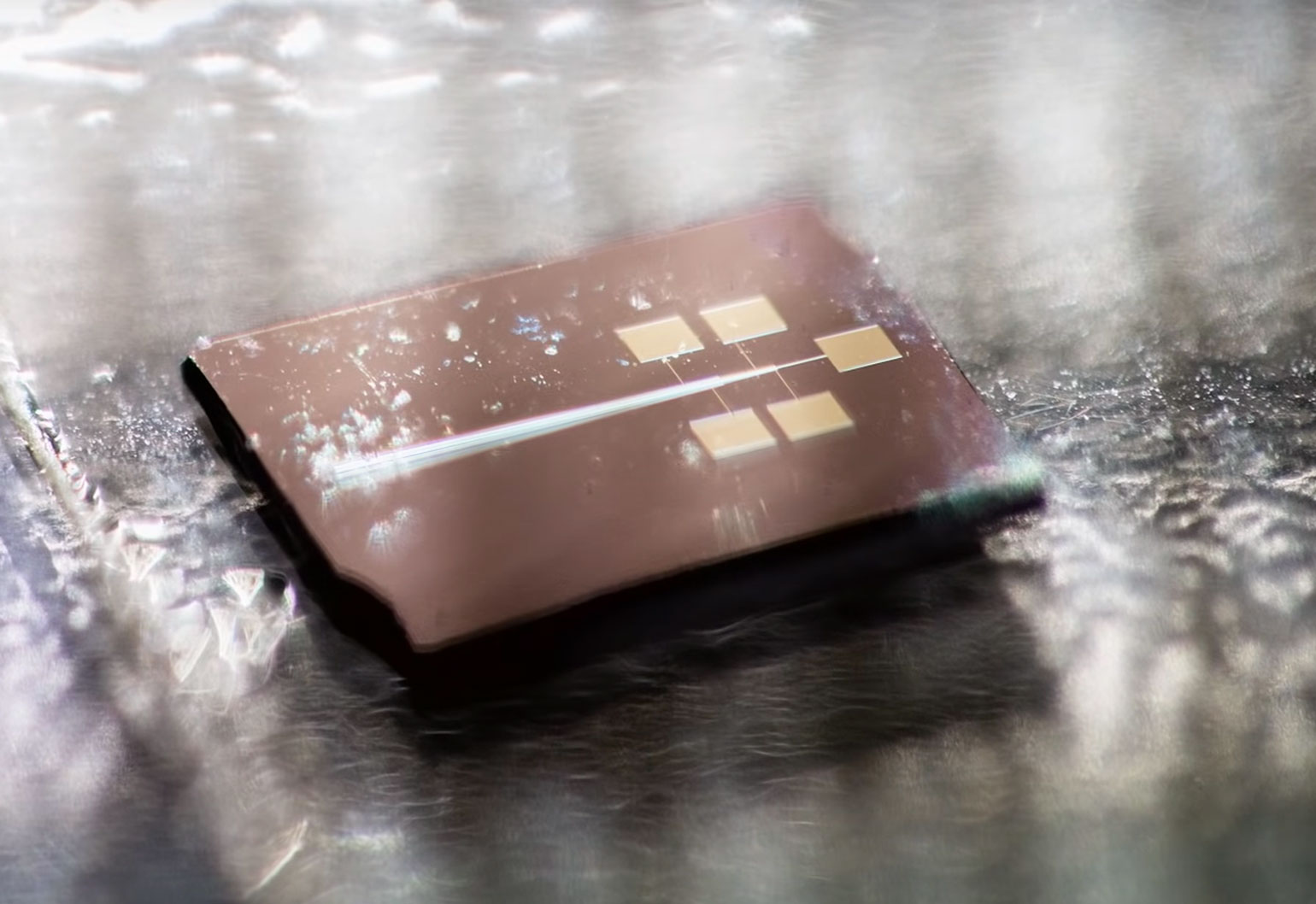
According to Australian National University (ANU) researcher and PhD student Ankur Sharma, the hybrid organic-inorganic semiconductor material can convert electricity to light very efficiently and be grown as thin as 2 nm or less – tens of thousands of times thinner than a human hair.
This makes it a candidate for future flexible electronic devices, Sharma told create.
“When you are at such low thicknesses, you have the capability to bend the material into any shape – much like a piece of paper,” he added.
While the semiconductor is not fully organic, Sharma hopes his research will pave the way to biodegradable materials to reduce the amount of electronic devices ending up as e-waste.
“We’re not there yet, but the organic component is a very good start,” Sharma said.
3D printing on an atomic scale
Sharma and his supervisor, Associate Professor Larry Lu, used a process called chemical vapour deposition to manufacture their semiconductor material.
This involved heating molecules at one end of a vacuum tube, and using a gas to deposit them one by one into a precise location on a chip.
“It’s very similar to 3D printing – growing everything from bottom up, but with atoms,” Sharma explained.
The hybrid organic-inorganic semiconductor combines the organic compound pentacene with a single molybdenum diselenide crystal.
Sharma explained the new material also has the potential to supercharge the processing power of mobile devices. Today’s phones use electricity alone to process information, but this new semiconductor is optoelectronic. This means it uses a mixture of light and electricity. As light is faster than electricity, processors using optoelectronic semiconductors would be much speedier than conventional processing tech.
“Mobile phones of today are similar to or better than the supercomputers of the 1990s. A mobile phone using optoelectronic semiconductors would be similar in processing power to today’s supercomputers,” Sharma said.
Sharma and Lu have a history of trailblazing. In 2016, they created what was believed to be the world’s thinnest lens from a single crystal of molybdenum disulphide.
Towards full biodegradability
While some devices use organic electronic components (such as OLEDs), Sharma said the majority of today’s semiconductors are inorganic. Therefore, researchers need to first demonstrate that organic materials are compatible with this technology.
There are also a number of challenges to overcome in the quest for an independent organic semiconductor that is fully sustainable.
“Working with the organic-inorganic hybrid was the best that we could achieve at this stage,” Sharma said.
The ANU team is now working to scale up production of their material, with a view to commercialisation in partnership with industry. Sharma said this could occur within three to five years, although there are still technical and market hurdles to be overcome.
Sharma has already polished his sales pitch. In September, he won the ANU Three Minute Thesis competition by explaining how his research could be implemented in lightning fast, flexible devices that won’t add to escalating e-waste.
And Sharma’s enthusiasm for this new generation of semiconductor materials is clear. He said his research team was aiming to improve their control over the quality of the materials further and use them in “as many actual working devices as we can”, ranging from flexible displays to processing devices or even solar cells.
“That’s the future direction: to find the right potential applications for these materials,” he said.