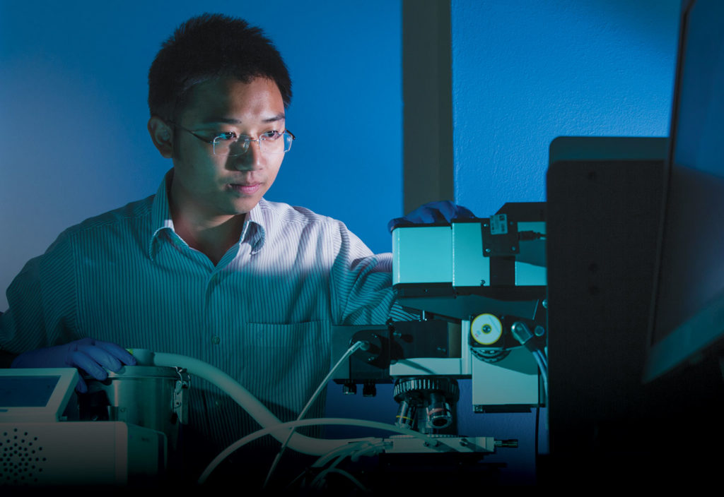
Engineers from the Australian National University (ANU) have developed a method that could help manufacturers spot defects in technology more easily and much earlier in the fabrication process.
The lead author of the study, Dr Hieu Nguyen from the ANU Research School of Electrical, Energy and Materials Engineering, said the method works by capturing high-resolution images of semiconductor materials, including many potential defects, within seconds.
Current methods measure point by point and can be slow and hugely impractical in the manufacturing environment.
“Before this research, to obtain an image with the resolution of 1000 by 1000 pixels, scientists in our lab had to perform one million point-by-point measurements, which took a whole week,” Nguyen said.
The work has been carried out in collaboration with scientists from the National Renewable Energy Laboratory in the United States.
It started when the team noticed that light emitting from various semiconductor materials, such as silicon, perovskite and thin films, had distinct qualities.
By using a scientific camera to capture the light, the images could then be used to extract in-depth information on how those materials work.
“We don’t capture all the light from an object,” Nguyen said.
“We capture only a specific colour that we need.”
Nguyen first noticed the light’s distinct qualities about six years ago, when he started his PhD.
“It is very different from the sunlight that we see every day. During this period, I also noticed that each part of the emitted light was very well correlated to a certain property of the materials,” he said.
He considered using a digital camera to capture the images and using cheap optical filters that cost a few hundred dollars to only let a specific part of the light enter the camera.
Doing so meant that instead of capturing a typical photo, images could be obtained that represent different parts of the light, giving researchers more information about materials.
So far, the team has demonstrated its research by capturing images of the optical bandgap, which determines numerous properties of semiconductors, including light absorption and electricity conduction, on perovskite solar cells made at ANU.
The technology could also be used for other devices made from semiconductors.
Picture perfect
Results from testing the ANU engineers’ defect detection process have been confirmed with other low-speed or low-resolution approaches. The next step will involve attracting industry to try the technology.
“It could be an advanced and fast defect characterisation tool for research and the industry,” Nguyen said.
“The technique could be helpful for many scientists and engineers in a few years.”
This article originally appeared as “Shine a light” in the August 2019 issue of create magazine.
